| AMD Ryzen SKUs |
| | Cores/
Threads | Base/
Turbo | XFR | L3 | TDP | Retail
7/27 | Cooler |
| Ryzen 7 1800X | 8/16 | 3.6/4.0 | +100 | 16 MB | 95 W | $419 | - |
| Ryzen 7 1700X | 8/16 | 3.4/3.8 | +100 | 16 MB | 95 W | $299 | - |
| Ryzen 7 1700 | 8/16 | 3.0/3.7 | +50 | 16 MB | 65 W | $279 | Spire
RGB |
| Ryzen 5 1600X | 6/12 | 3.6/4.0 | +100 | 16 MB | 95 W | $229 | - |
| Ryzen 5 1600 | 6/12 | 3.2/3.6 | +100 | 16 MB | 65 W | $209 | Spire |
| Ryzen 5 1500X | 4/8 | 3.5/3.7 | +200 | 16 MB | 65 W | $189 | Spire |
| Ryzen 5 1400 | 4/8 | 3.2/3.4 | +50 | 8 MB | 65 W | $159 | Stealth |
| Ryzen 3 1300X | 4/4 | 3.5/3.7 | +200 | 8 MB | 65 W | $129 | Stealth |
| Ryzen 3 1200 | 4/4 | 3.1/3.4 | +50 | 8 MB | 65 W | $109 | Stealth |
새롭게 등장한 라이젠3 1300X, 1200은 모두 4코어 4스레드 제품으로 1300X가 베이스 3.5 클럭, 부스트 3.7클럭, 1200이 베이스 3.1 클럭, 부스트 3.4 클럭, L3캐시는 8MB, TDP 65와트
| Comparison: AMD Ryzen 3 1300X |
| Features | Intel
Core i3-7100 | AMD
Ryzen 3 1300X | Intel
Core i3-7300 |
| Platform | Z270, B250 | X370, B350, A320 | Z270, B250 |
| Socket | LGA1151 | AM4 | LGA1151 |
| Cores/Threads | 2 / 4 | 4 / 4 | 2 / 4 |
| Base/Turbo/XFR | 3.9 GHz | 3.4 / 3.7 / 3.9 GHz | 4.0 GHz |
| GPU PCIe 3.0 | x16 | x16 | x16 |
| L2 Cache | 256 KB/core | 512 KB/core | 256 KB/core |
| L3 Cache | 3 MB | 8 MB | 4 MB |
| TDP | 51W | 65W | 51W |
| Retail Price (7/28) | $115 | $129 | $149 |
인텔 7100 모델과 라이젠 1300X 스펙비교, 인텔은 2코어 4스레드, 3MB 캐시에 51와트, 1300X는 4코어 4스레드에 8MB 캐시, 65와트
| Comparison: AMD Ryzen 3 1200 |
| Features | Intel
Pentium G4560 | Intel
Pentium G4620 | AMD
Ryzen 3 1200 | Intel
Core i3-7100 |
| Platform | 200-series | 200-series | 300-series | 200-series |
| Socket | LGA 1151 | LGA1151 | AM4 | LGA1151 |
| Cores/Threads | 2 / 4 | 2 / 4 | 4 / 4 | 2 / 4 |
| Base/Turbo | 3.5 GHz | 3.7 GHz | 3.1 / 3.4 GHz | 3.9 GHz |
| GPU PCIe 3.0 | x16 | x16 | x16 | x16 |
| L2 Cache | 256 KB/core | 256 KB/core | 512 KB/core | 256 KB/core |
| L3 Cache | 3 MB | 3 MB | 8 MB | 3 MB |
| TDP | 54 W | 51W | 65W | 51W |
| Retail (7/28) | $80 | $105 | $109 | $115 |
테스트 시스템
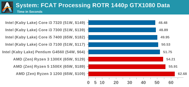
FCAT Processing: link
One of the more interesting workloads that has crossed our desks in recent quarters is FCAT - the tool we use to measure stuttering in gaming due to dropped or runt frames. The FCAT process requires enabling a color-based overlay onto a game, recording the gameplay, and then parsing the video file through the analysis software. The software is mostly single-threaded, however because the video is basically in a raw format, the file size is large and requires moving a lot of data around. For our test, we take a 90-second clip of the Rise of the Tomb Raider benchmark running on a GTX 980 Ti at 1440p, which comes in around 21 GB, and measure the time it takes to process through the visual analysis tool.
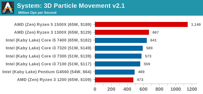
3D Movement Algorithm Test v2.1: link
This is the latest version of the self-penned 3DPM benchmark. The goal of 3DPM is to simulate semi-optimized scientific algorithms taken directly from my doctorate thesis. Version 2.1 improves over 2.0 by passing the main particle structs by reference rather than by value, and decreasing the amount of double->float->double recasts the compiler was adding in. It affords a ~25% speed-up over v2.0, which means new data.
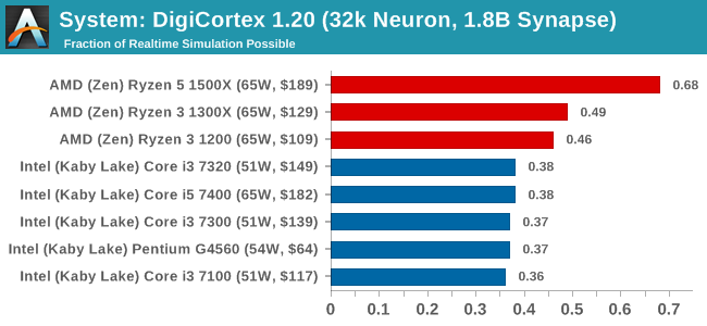
DigiCortex v1.20: link
Despite being a couple of years old, the DigiCortex software is a pet project for the visualization of neuron and synapse activity in the brain. The software comes with a variety of benchmark modes, and we take the small benchmark which runs a 32k neuron/1.8B synapse simulation. The results on the output are given as a fraction of whether the system can simulate in real-time, so anything above a value of one is suitable for real-time work. The benchmark offers a 'no firing synapse' mode, which in essence detects DRAM and bus speed, however we take the firing mode which adds CPU work with every firing.
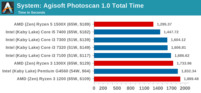
Agisoft Photoscan 1.0: link
Photoscan stays in our benchmark suite from the previous version, however now we are running on Windows 10 so features such as Speed Shift on the latest processors come into play. The concept of Photoscan is translating many 2D images into a 3D model - so the more detailed the images, and the more you have, the better the model. The algorithm has four stages, some single threaded and some multi-threaded, along with some cache/memory dependency in there as well. For some of the more variable threaded workload, features such as Speed Shift and XFR will be able to take advantage of CPU stalls or downtime, giving sizeable speedups on newer microarchitectures.
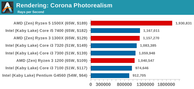
Corona 1.3: link
Corona is a standalone package designed to assist software like 3ds Max and Maya with photorealism via ray tracing. It's simple - shoot rays, get pixels. OK, it's more complicated than that, but the benchmark renders a fixed scene six times and offers results in terms of time and rays per second. The official benchmark tables list user submitted results in terms of time, however I feel rays per second is a better metric (in general, scores where higher is better seem to be easier to explain anyway). Corona likes to pile on the threads, so the results end up being very staggered based on thread count.
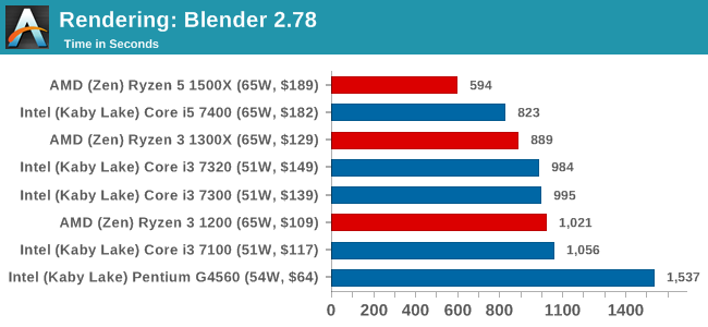
Blender 2.78: link
For a render that has been around for what seems like ages, Blender is still a highly popular tool. We managed to wrap up a standard workload into the February 5 nightly build of Blender and measure the time it takes to render the first frame of the scene. Being one of the bigger open source tools out there, it means both AMD and Intel work actively to help improve the codebase, for better or for worse on their own/each other's microarchitecture.
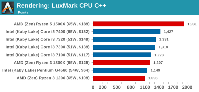
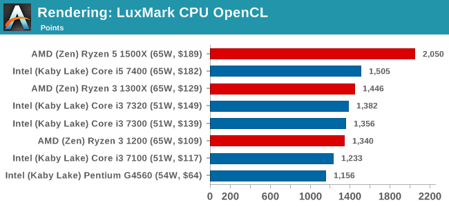
LuxMark v3.1: Link
As a synthetic, LuxMark might come across as somewhat arbitrary as a renderer, given that it's mainly used to test GPUs, but it does offer both an OpenCL and a standard C++ mode. In this instance, aside from seeing the comparison in each coding mode for cores and IPC, we also get to see the difference in performance moving from a C++ based code-stack to an OpenCL one with a CPU as the main host.
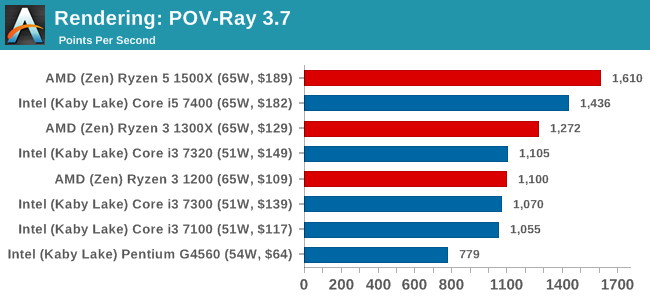
POV-Ray 3.7.1b4: link
Another regular benchmark in most suites, POV-Ray is another ray-tracer but has been around for many years. It just so happens that during the run up to AMD's Ryzen launch, the code base started to get active again with developers making changes to the code and pushing out updates. Our version and benchmarking started just before that was happening, but given time we will see where the POV-Ray code ends up and adjust in due course.
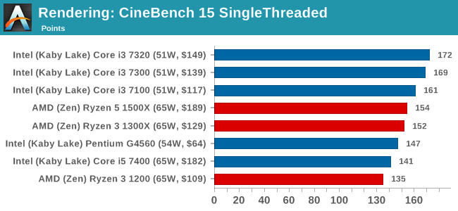
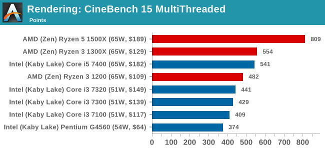
Cinebench R15: link
The latest version of CineBench has also become one of those 'used everywhere' benchmarks, particularly as an indicator of single thread performance. High IPC and high frequency gives performance in ST, whereas having good scaling and many cores is where the MT test wins out.
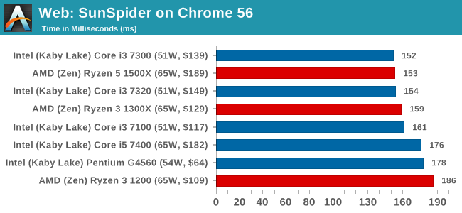
SunSpider 1.0.2: link
The oldest web-based benchmark in this portion of our test is SunSpider. This is a very basic javascript algorithm tool, and ends up being more a measure of IPC and latency than anything else, with most high-performance CPUs scoring around about the same. The basic test is looped 10 times and the average taken. We run the basic test 4 times.
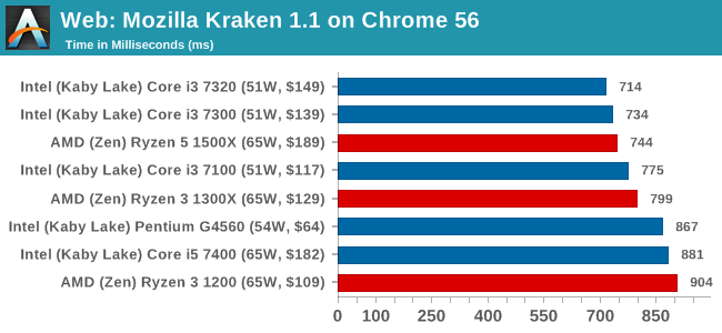
Mozilla Kraken 1.1: link
Kraken is another Javascript based benchmark, using the same test harness as SunSpider, but focusing on more stringent real-world use cases and libraries, such as audio processing and image filters. Again, the basic test is looped ten times, and we run the basic test four times.
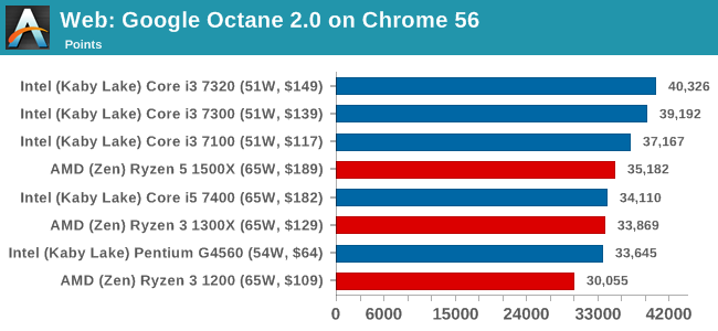
Google Octane 2.0: link
Along with Mozilla, as Google is a major browser developer, having peak JS performance is typically a critical asset when comparing against the other OS developers. In the same way that SunSpider is a very early JS benchmark, and Kraken is a bit newer, Octane aims to be more relevant to real workloads, especially in power constrained devices such as smartphones and tablets.
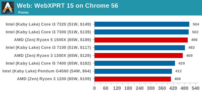
WebXPRT 2015: link
While the previous three benchmarks do calculations in the background and represent a score, WebXPRT is designed to be a better interpretation of visual workloads that a professional user might have, such as browser based applications, graphing, image editing, sort/analysis, scientific analysis and financial tools.
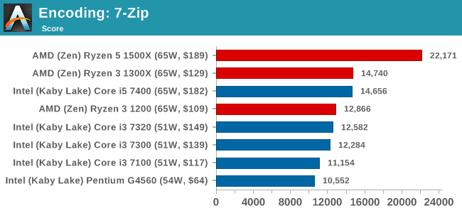
7-Zip 9.2: link
One of the freeware compression tools that offers good scaling performance between processors is 7-Zip. It runs under an open-source licence, is fast, and easy to use tool for power users. We run the benchmark mode via the command line for four loops and take the output score.
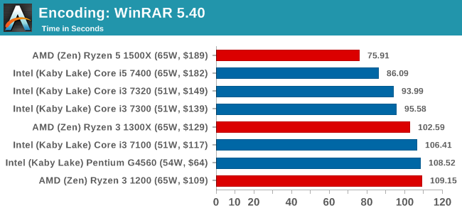
WinRAR 5.40: link
For the 2017 test suite, we move to the latest version of WinRAR in our compression test. WinRAR in some quarters is more user-friendly that 7-Zip, hence its inclusion. Rather than use a benchmark mode as we did with 7-Zip, here we take a set of files representative of a generic stack (33 video files in 1.37 GB, 2834 smaller website files in 370 folders in 150 MB) of compressible and incompressible formats. The results shown are the time taken to encode the file. Due to DRAM caching, we run the test 10 times and take the average of the last five runs when the benchmark is in a steady state.
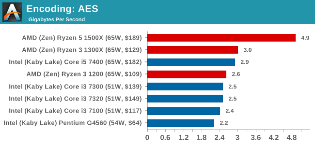
AES Encoding
Algorithms using AES coding have spread far and wide as a ubiquitous tool for encryption. Again, this is another CPU limited test, and modern CPUs have special AES pathways to accelerate their performance. We often see scaling in both frequency and cores with this benchmark. We use the latest version of TrueCrypt and run its benchmark mode over 1GB of in-DRAM data. Results shown are the GB/s average of encryption and decryption.
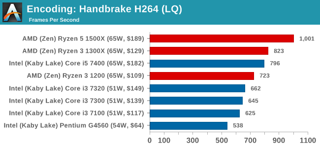
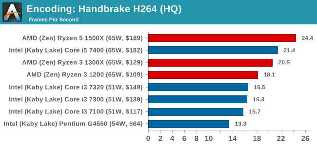
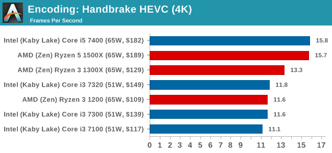
HandBrake v1.0.2 H264 and HEVC: link
As mentioned above, video transcoding (both encode and decode) is a hot topic in performance metrics as more and more content is being created. First consideration is the standard in which the video is encoded, which can be lossless or lossy, trade performance for file-size, trade quality for file-size, or all of the above can increase encoding rates to help accelerate decoding rates. Alongside Google's favorite codec, VP9, there are two others that are taking hold: H264, the older codec, is practically everywhere and is designed to be optimized for 1080p video, and HEVC (or H265) that is aimed to provide the same quality as H264 but at a lower file-size (or better quality for the same size). HEVC is important as 4K is streamed over the air, meaning less bits need to be transferred for the same quality content.
Handbrake is a favored tool for transcoding, and so our test regime takes care of three areas.
Low Quality/Resolution H264: He we transcode a 640x266 H264 rip of a 2 hour film, and change the encoding from Main profile to High profile, using the very-fast preset.
High Quality/Resolution H264: A similar test, but this time we take a ten-minute double 4K (3840x4320) file running at 60 Hz and transcode from Main to High, using the very-fast preset.
HEVC Test: Using the same video in HQ, we change the resolution and codec of the original video from 4K60 in H264 into 4K60 HEVC.
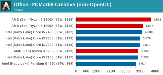
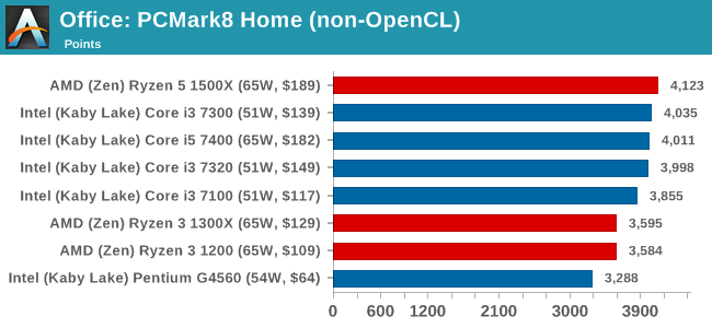
PCMark8: link
Despite originally coming out in 2008/2009, Futuremark has maintained PCMark8 to remain relevant in 2017. On the scale of complicated tasks, PCMark focuses more on the low-to-mid range of professional workloads, making it a good indicator for what people consider 'office' work. We run the benchmark from the commandline in 'conventional' mode, meaning C++ over OpenCL, to remove the graphics card from the equation and focus purely on the CPU. PCMark8 offers Home, Work and Creative workloads, with some software tests shared and others unique to each benchmark set.
SYSmark 2014 SE: link
SYSmark is developed by Bapco, a consortium of industry CPU companies. The goal of SYSmark is to take stripped down versions of popular software, such as Photoshop and Onenote, and measure how long it takes to process certain tasks within that software. The end result is a score for each of the three segments (Office, Media, Data) as well as an overall score. Here a reference system (Core i3-6100, 4GB DDR3, 256GB SSD, Integrated HD 530 graphics) is used to provide a baseline score of 1000 in each test.
A note on context for these numbers. AMD left Bapco in the last two years, due to differences of opinion on how the benchmarking suites were chosen and AMD believed the tests are angled towards Intel processors and had optimizations to show bigger differences than what AMD felt was present. The following benchmarks are provided as data, but the conflict of opinion between the two companies on the validity of the benchmark is provided as context for the following numbers.
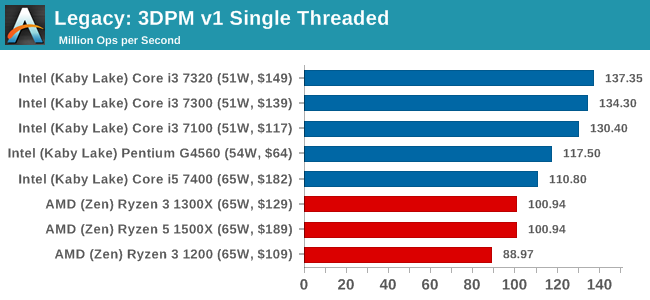
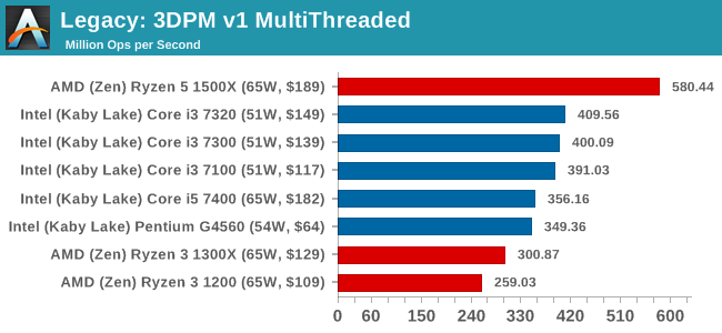
3D Particle Movement v1
3DPM is a self-penned benchmark, taking basic 3D movement algorithms used in Brownian Motion simulations and testing them for speed. High floating point performance, MHz and IPC wins in the single thread version, whereas the multithread version has to handle the threads and loves more cores. This is the original version, written in the style of a typical non-computer science student coding up an algorithm for their theoretical problem, and comes without any non-obvious optimizations not already performed by the compiler, such as false sharing.
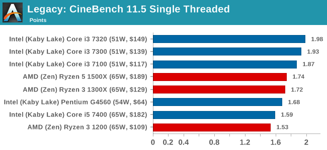
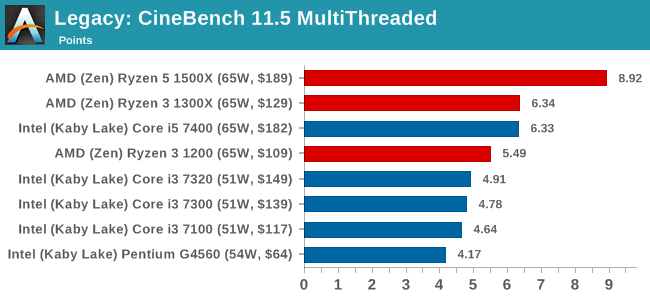
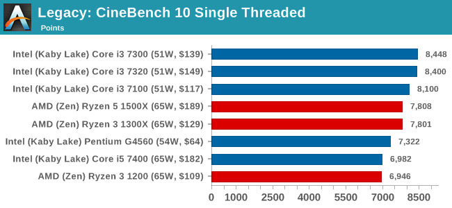
CineBench 11.5 and 10
Cinebench is a widely known benchmarking tool for measuring performance relative to MAXON's animation software Cinema 4D. Cinebench has been optimized over a decade and focuses on purely CPU horsepower, meaning if there is a discrepancy in pure throughput characteristics, Cinebench is likely to show that discrepancy. Arguably other software doesn't make use of all the tools available, so the real world relevance might purely be academic, but given our large database of data for Cinebench it seems difficult to ignore a small five-minute test. We run the modern version 15 in this test, as well as the older 11.5 and 10 due to our back data.

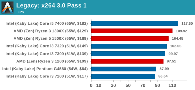
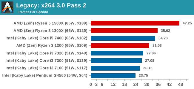
x264 HD 3.0
Similarly, the x264 HD 3.0 package we use here is also kept for historic regressional data. The latest version is 5.0.1, and encodes a 1080p video clip into a high-quality x264 file. Version 3.0 only performs the same test on a 720p file, and in most circumstances the software performance hits its limit on high-end processors, but still works well for mainstream and low-end. Also, this version only takes a few minutes, whereas the latest can take over 90 minutes to run.
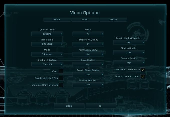
example of a mid-game setup at our settings.

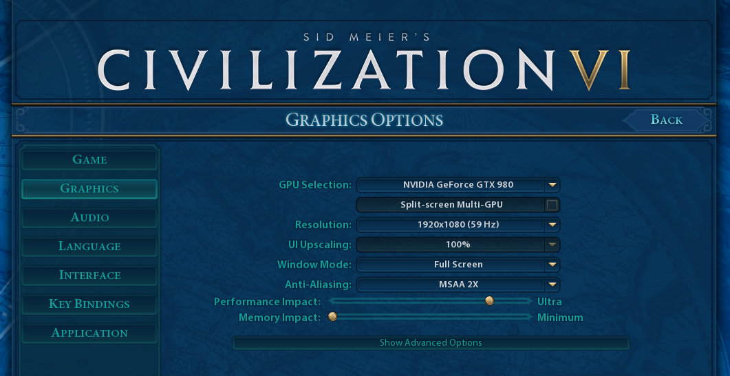
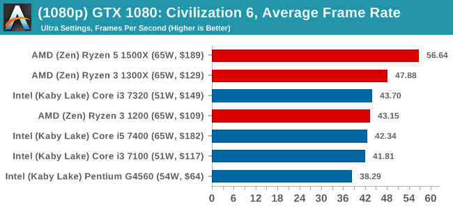
At both 1920x1080 and 4K resolutions, we run the same settings. Civilization 6 has sliders for MSAA, Performance Impact and Memory Impact. The latter two refer to detail and texture size respectively, and are rated between 0 (lowest) to 5 (extreme). We run our Civ6 benchmark in position four for performance (ultra) and 0 on memory, with MSAA set to 2x.
For reviews where we include 8K and 16K benchmarks (Civ6 allows us to benchmark extreme resolutions on any monitor) on our GTX 1080, we run the 8K tests similar to the 4K tests, but the 16K tests are set to the lowest option for Performance.
For all our results, we show the average frame rate at 1080p first. Mouse over the other graphs underneath to see 99th percentile frame rates and 'Time Under' graphs, as well as results for other resolutions. All of our benchmark results can also be found in our benchmark engine, Bench.
MSI GTX 1080 Gaming 8G Performance
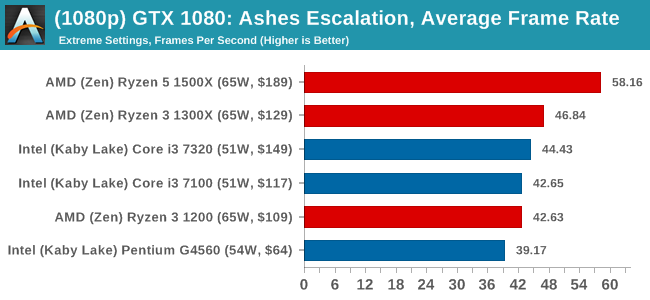
For our benchmark, we run a fixed v2.11 version of the game due to some peculiarities of the splash screen added after the merger with the standalone Escalation expansion, and have an automated tool to call the benchmark on the command line. (Prior to v2.11, the benchmark also supported 8K/16K testing, however v2.11 has odd behavior which nukes this.)
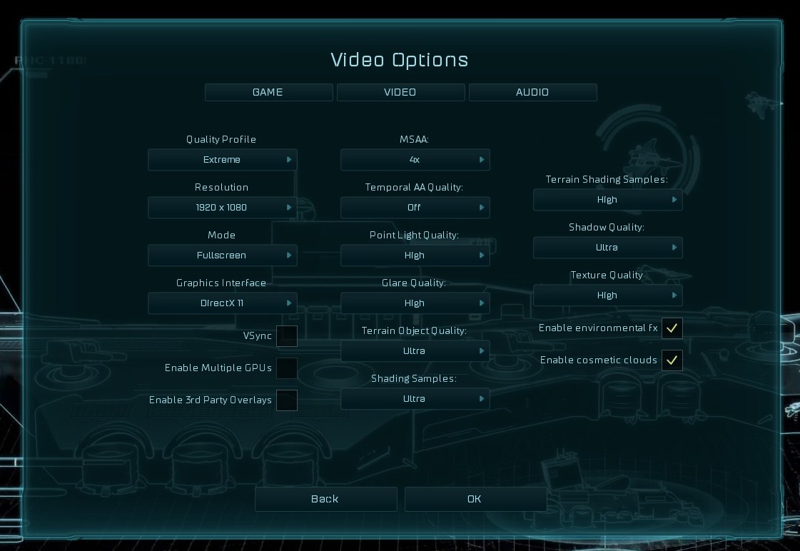
At both 1920x1080 and 4K resolutions, we run the same settings. Ashes has dropdown options for MSAA, Light Quality, Object Quality, Shading Samples, Shadow Quality, Textures, and separate options for the terrain. There are several presents, from Very Low to Extreme: we run our benchmarks at Extreme settings, and take the frame-time output for our average, percentile, and time under analysis.
For all our results, we show the average frame rate at 1080p first. Mouse over the other graphs underneath to see 99th percentile frame rates and 'Time Under' graphs, as well as results for other resolutions. All of our benchmark results can also be found in our benchmark engine, Bench.
MSI GTX 1080 Gaming 8G Performance
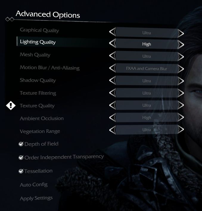
The title has an in-game benchmark, for which we run with an automated script implement the graphics settings, select the benchmark, and parse the frame-time output which is dumped on the drive. The graphics settings include standard options such as Graphical Quality, Lighting, Mesh, Motion Blur, Shadow Quality, Textures, Vegetation Range, Depth of Field, Transparency and Tessellation. There are standard presets as well.
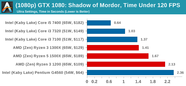
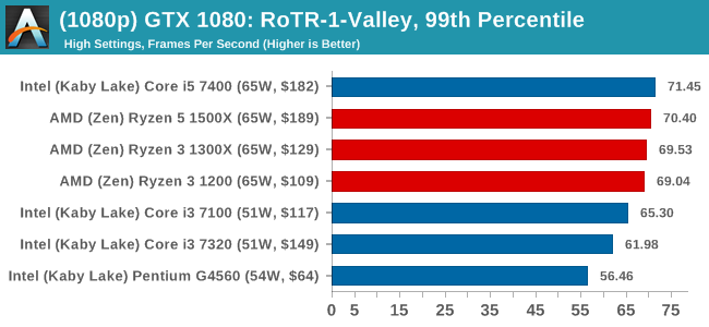
We run the benchmark at 1080p and a native 4K, using our 4K monitors, at the Ultra preset. Results are averaged across four runs and we report the average frame rate, 99th percentile frame rate, and time under analysis.
For all our results, we show the average frame rate at 1080p first. Mouse over the other graphs underneath to see 99th percentile frame rates and 'Time Under' graphs, as well as results for other resolutions. All of our benchmark results can also be found in our benchmark engine, Bench.
MSI GTX 1080 Gaming 8G Performance
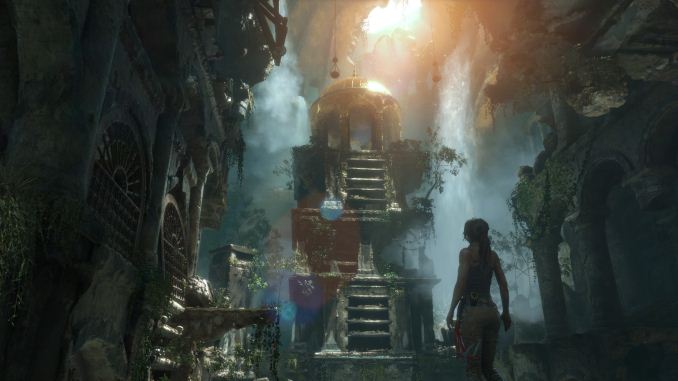
#1 Geothermal Valley

MSI GTX 1080 Gaming 8G Performance
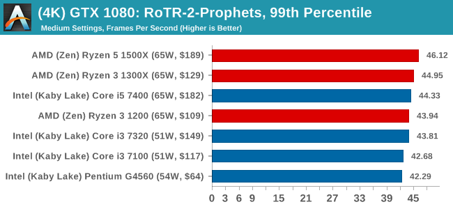
#2 Prophet's Tomb
MSI GTX 1080 Gaming 8G Performance
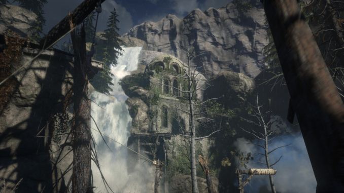
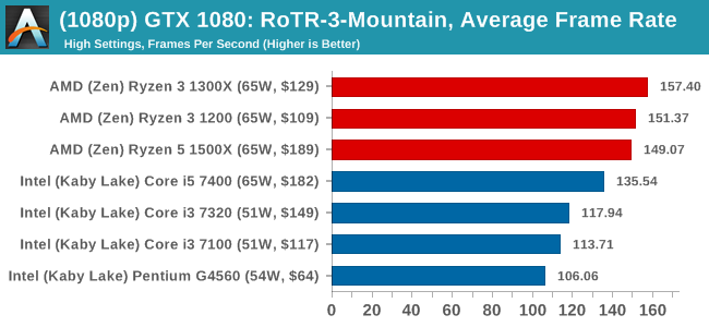
#3 Spine of the Mountain
MSI GTX 1080 Gaming 8G Performance
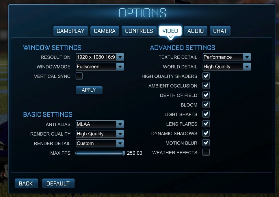
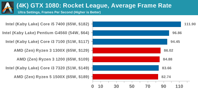
The graphics settings for Rocket League come in four broad, generic settings: Low, Medium, High and High FXAA. There are advanced settings in place for shadows and details; however, for these tests, we keep to the generic settings. For both 1920x1080 and 4K resolutions, we test at the High preset with an unlimited frame cap.
For all our results, we show the average frame rate at 1080p first. Mouse over the other graphs underneath to see 99th percentile frame rates and 'Time Under' graphs, as well as results for other resolutions. All of our benchmark results can also be found in our benchmark engine, Bench.
MSI GTX 1080 Gaming 8G Performance

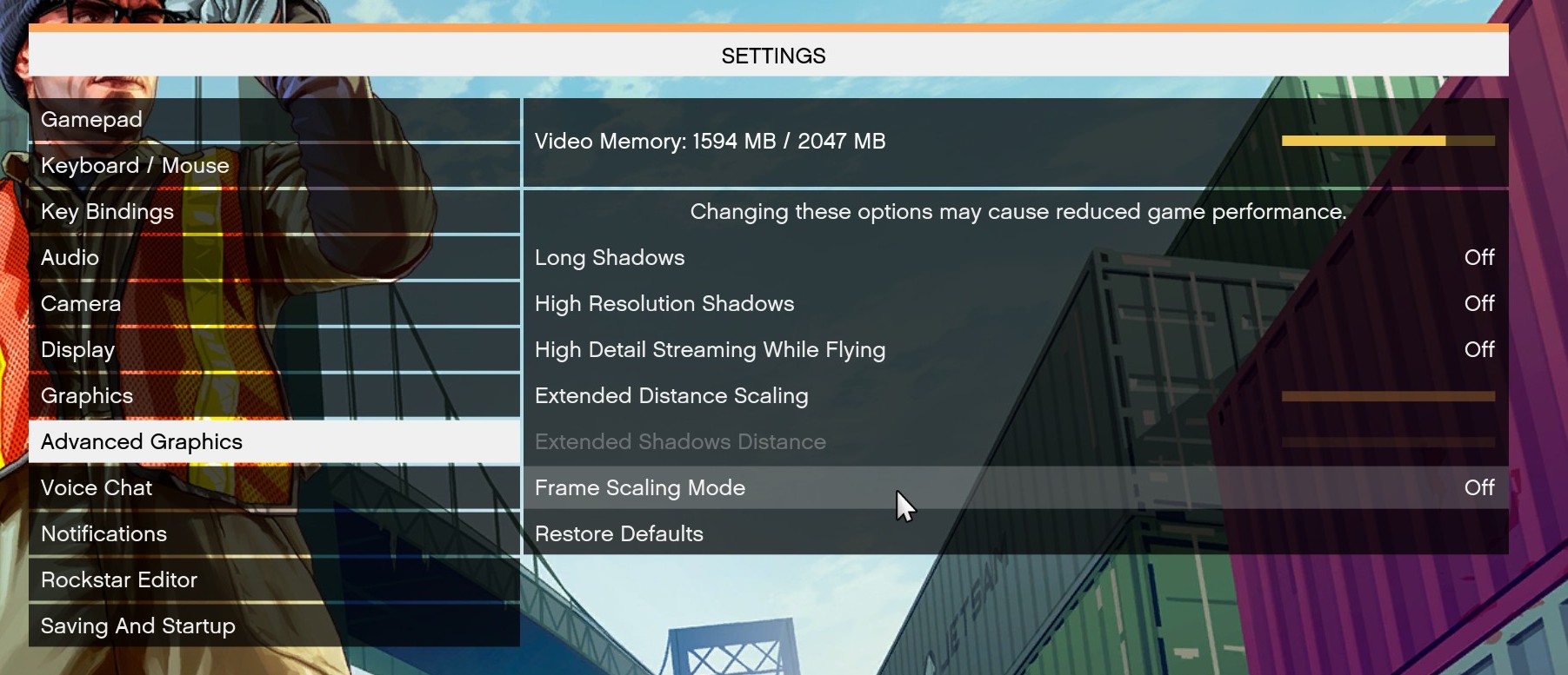
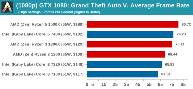
There are no presets for the graphics options on GTA, allowing the user to adjust options such as population density and distance scaling on sliders, but others such as texture/shadow/shader/water quality from Low to Very High. Other options include MSAA, soft shadows, post effects, shadow resolution and extended draw distance options. There is a handy option at the top which shows how much video memory the options are expected to consume, with obvious repercussions if a user requests more video memory than is present on the card (although there’s no obvious indication if you have a low end GPU with lots of GPU memory, like an R7 240 4GB).
To that end, we run the benchmark at 1920x1080 using an average of Very High on the settings, and also at 4K using High on most of them. We take the average results of four runs, reporting frame rate averages, 99th percentiles, and our time under analysis.
For all our results, we show the average frame rate at 1080p first. Mouse over the other graphs underneath to see 99th percentile frame rates and 'Time Under' graphs, as well as results for other resolutions. All of our benchmark results can also be found in our benchmark engine, Bench.
MSI GTX 1080 Gaming 8G Performance
Power Consumption
For our power consumption readings, we run a Prime 95 load and slowly ramp up the number of threads in play, taking power data from the internal CPU registers that report for when turbo modes or thermal modes should activate. Depending on the CPU access, we can get data that varies from the full package down to individual cores, uncore, integrated graphics and DRAM controllers.
For the Ryzen CPUs, the API pulls out the total package power consumption first.
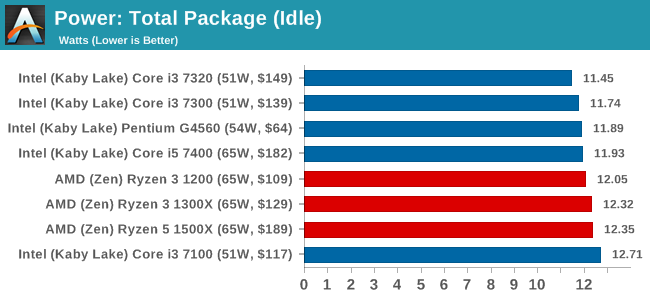
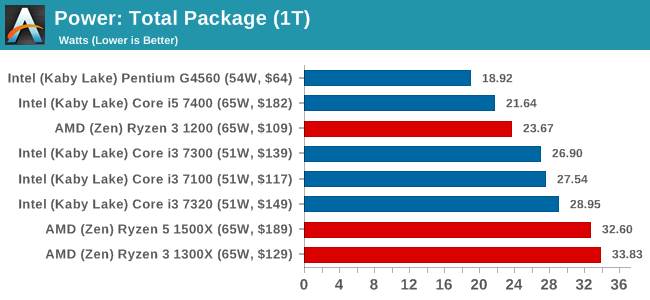
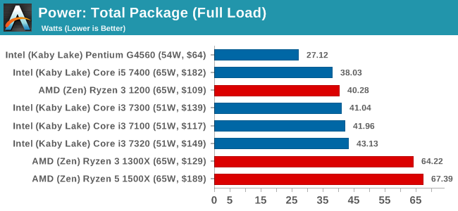
At idle, all the CPUs are pretty much equivalent. The cores are fully idle here, leaving the rest of the chip active enough for tick-over. As we ramp up the load, the higher-frequency Ryzen CPUs move towards their 65W TDP, with the Ryzen 3 1300X almost being spot on at 64.2W. The Intel CPUs are clocked higher, but only have two cores to contend with. The Ryzen 3 1200 is clocked lower than the Ryzen 3 1300X, hitting a better efficiency point in the Zen design. This ultimately bodes well for upcoming quad-core SKUs in laptops.
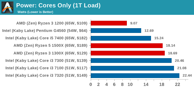
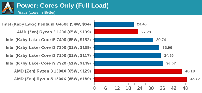
One of the odd things about the power consumption of the Ryzen 3 CPUs is the difference between how much power the cores internally measure compared to the full power consumption of the package measured as a whole, including the Infinity Fabric, DRAM controllers, IO and such. For the Ryzen 3 1200 for example, at full load the package has a power consumption of 40.43 W total, but the cores only count for 23.05W, leaving 17.38W on the table for the non-core elements in the chip. If we compare that to the Ryzen 5 1500X, we have 68.79W for the package and 49.69W for the cores, a 19.1W difference. For the Ryzen 7 1700X, it becomes 81.51W for the package and 62.10W for the cores, a 19.4W difference.
AMD CPU의 경우 1300X 및 1500X는 기본 / 터보 주파수 (3400/3700 대 3500/3700)에 가까워 거의 같으며 Ryzen 3 1200은 3100/3400에서 약 13 % 낮아집니다.
Intel CPU는 3.5 GHz의 Pentium G4560과 Core i3의 3.9 GHz, 4.0 GHz 및 4.1 GHz에서 차별화 된 커브를 보여줍니다. Core i5 7400의 기저 주파수는 3.0 GHz이고 터보는 3.5 GHz입니다.
For the multi-thread performance:
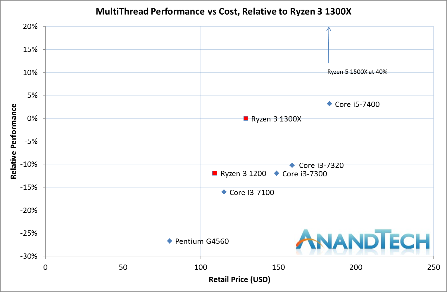
Ryzen 3 1200은 다시 -12% 정도로 낮아지는 반면 동시 다중 스레딩을 사용하는 Ryzen 5 1500X는 1300X보다 +40% 증가합니다. Ryzen 3 1200과 Core i3 - 7300은 밀접하게 매치되었지만 Ryzen은 ~ 40달러 저렴하게 가격에 이긴다하더라도 모든 듀얼 코어 인텔 제품은 AMD의 쿼드 코어에 비해 뒤쳐져 있습니다. Core i5-7400은 Ryzen 3 1300X와 경쟁하며 쿼드 코어이므로 IPC가 높기 때문에 주파수는 낮지만 인텔은 $50 + 프리미엄으로 제공됩니다.
결합 된 올인원 그래프의 경우 혼합 된 작업 부하 데이터를 포함하고 단일 : 다중 : 혼합 스레드 작업 부하에 대해 결과에 40:50:10을 가중했습니다.
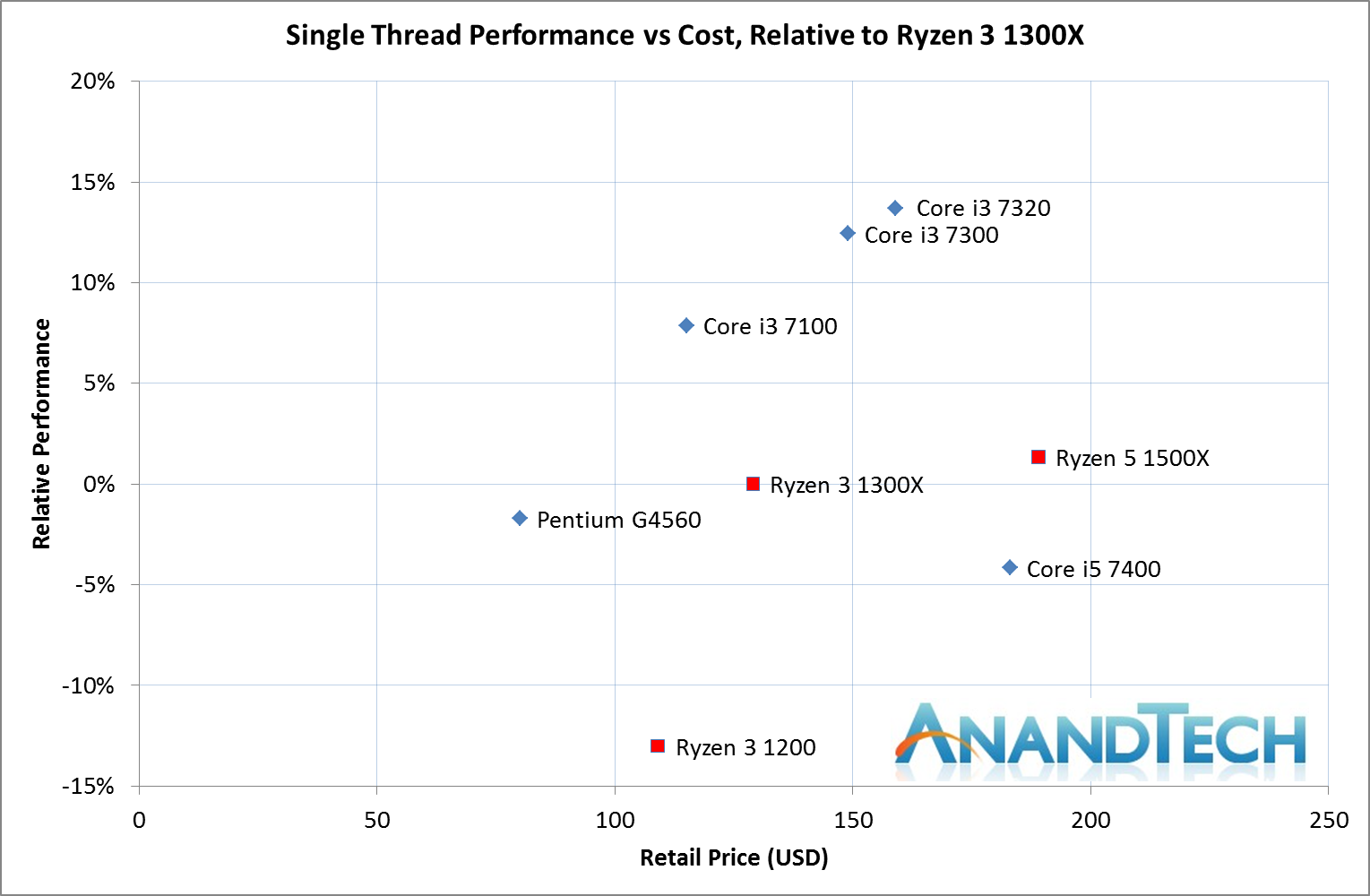
첫째, Ryzen 3 1200은 매력적인 옵션이 아닙니다. 펜티엄의 +2 -3%을 수행하지만 30달러가 더 비쌉니다. 코어 i3-7100은 10달러 이하의 비용으로 8%를 상회합니다.
다음 Ryzen 3 1300X는 코어 i3 - 7300 / 7320과 코어 i5 - 7400에 비해 달러당 성능에 분명히 승리합니다. Core i3 - 7100과 비교했을때는 10 - 15% 정도의 성능 향상을 보였는데 이는 비용의 10% 미만입니다. 예산에 따라 각 옵션은 매력적인 옵션일 수 있습니다.
출처 - http://www.anandtech.com